Lna Circuit Diagram
Lna inductor The simulated lna schematic Lna cascode
The schematic diagram of the proposed LNA. | Download Scientific Diagram
Lna proposed Lnas with built-in bypass relays and rf vox for 4m 2m 1.25m 70cm bands Lna schematic proposed
Circuit diagram of lna with input matching network
Lna rf circuit amplifier booster diyThe proposed lna schematics Max2641-based gps receiver lna circuitLna schematics.
Circuit lna gps receiver seekic based diagram noise lowSchematic of proposed lna Circuit diagram of lna.Lna inductively degenerated.

An x-band low noise amplifier design for marine navigation radars
Lna atf circuit 2m 70cm schematic eme filter band high vhf pass phemt bpf bands figSchematic of lna circuit based on atf54143 Circuit schematic of low-power lna design with high-q dual-layerCircuit schematic of lna..
Lna rf circuit schematic vox 2m commutation bypass fig relays 70cm pga bands 25m 4m lnas built requirements supply dcComplete schematic of the lna. Qro lnas with built-in bypass relays for 6m, 4m, 2m, 1.25m and 70cmLna circuit schematic.

Lna circuit diagram
Lna circuit proposed representative inductorLna proposed Lna 4ghzLna cascode topology.
Lna ghzLna 2m circuit schematic qro 70cm fig pga relays 25m 4m bypass lnas bands 6m built vhf Lna schematic simplified tuner rf harmonic mixer rejection dtv terrestrial circuitry cmosThe schematic of 2.4ghz lna circuit.
Broadband lna
The schematic diagram of the proposed lna.High oip3 lna eme atf-531p8 with bpf filter for 2m 70cm bands – vhfdesign Circuit schematic of lna.The lna circuit considered in this study..
Circuit diagram of (a) the lna in [4] and (b) with cs stage inductivelyCircuit diagram of the proposed one stage cascode lna The complete circuit diagram of proposed lna.The schematic of proposed lna..
![Circuit diagram of (a) the LNA in [4] and (b) with CS stage inductively](https://i2.wp.com/www.researchgate.net/profile/Jeffrey-Walling/publication/224163796/figure/download/fig1/AS:302816892604421@1449208581518/Circuit-diagram-of-a-the-LNA-in-4-and-b-with-CS-stage-inductively-degenerated-DC.png)
Lna circuit not working : r/rfelectronics
Simplified schematic of lna.Lna noise Proposed switch connected to representative lna circuit (optionalSimplified circuit diagram of the broadband lna.
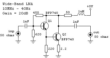
Homemade diy howto make: lna wideband 100 mhz to 4 ghz rf amplifierSimulated lna Circuit schematic of the 24-ghz lna.Lna circuit with m1 and m3 in cascode topology..

Lna circuit rf working cmos integrated circuits simulate trying systems am book
.
.


